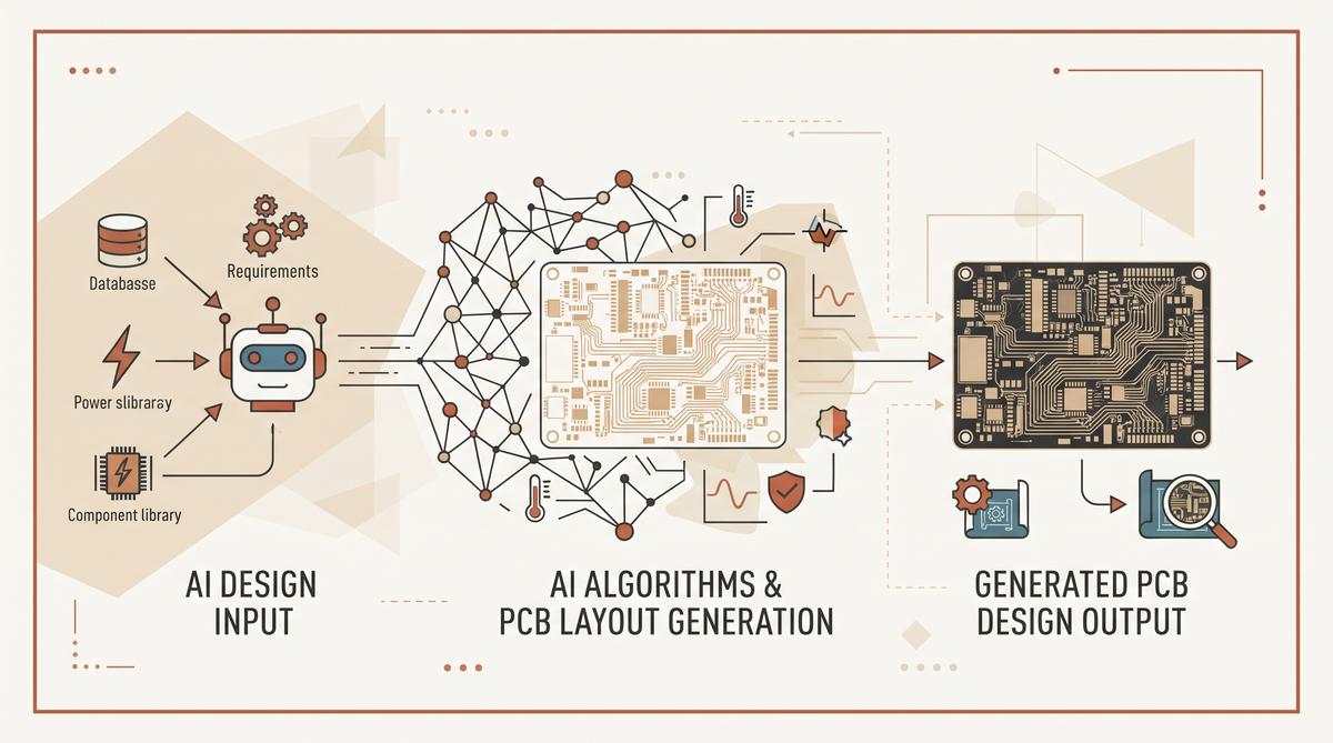
In September 2026, a Hacker News thread titled “Can AI now design PCBs that just work?” drew thousands of comments from working engineers within days. Hackaday picked up the discussion on September 5, 2026, and the consensus was blunt. AI can draft, suggest, and accelerate — but it cannot own manufacturing-ready signoff.
TL;DR: A September 2026 Hacker News debate examined whether AI can design circuit boards yet. The consensus: frontier models like GPT-6 Astra help with drafting and component selection, but cannot own manufacturing-ready signoff. Engineers remain in charge of final validation before a board goes to fabrication.
Can AI Actually Design a PCB Today?
No — not end to end. Frontier AI models can produce plausible schematics, suggest components, and even generate KiCad source files, but a manufacturing-ready board requires validation steps no current model can reliably perform. Ken Ashe, writing on the AI Application Builder blog, frames the useful distinction: drafting help versus engineering judgment versus manufacturing signoff (source: kenashe.ai).
What does “designing” even mean here? A PCB project spans schematic capture, component selection, layout, routing, design rule checks, signal integrity analysis, thermal review, and finally fabrication files. AI touches the first few stages meaningfully. The later stages are where it falls apart.
So the honest answer is partial. AI assists with the front of the workflow. Engineers still own the back. The Hackaday discussion reflected exactly this split, with hobbyists reporting genuine wins on simple boards and professionals rejecting the idea of unsupervised output for anything heading to a fab house (source: Hackaday).
Think of it as a very fast, occasionally overconfident junior designer.
What Sparked the Debate on Hacker News?
The trigger was a wave of demos showing frontier models generating complete PCB projects from natural-language prompts. A TechPlanet post titled “AI Can Now Design Circuit Boards” claimed a significant milestone: frontier AI models demonstrating the ability to design functional boards (source: TechPlanet). That claim landed on Hacker News, and engineers stress-tested it.
The backlash was fast. Commenters who actually tried the workflows reported that generated boards “worked” only in the loosest sense — simple LED blinkers, dev-board breakouts, textbook regulator circuits. Anything involving mixed-signal layout, controlled impedance, or EMC compliance failed quietly. A PromptZone roundup of the thread catalogued reported benchmarks and direct comparisons to traditional EDA tooling, finding the gap between demo and production far wider than promotional posts suggested (source: PromptZone).
The debate matters because it exposed a pattern we’ve seen elsewhere in AI. Spectacular demos. Then quiet failure on real constraints.
Why does this keep happening? Because PCB design punishes errors you cannot see in a schematic.
Which Parts of PCB Design Can AI Handle Well?
AI genuinely helps with several front-end tasks. According to the Hacker News discussion and the EEBench analysis of what current models can build, these are the areas where models add real value (source: EEBench):
- Generating draft schematics for common topologies like power supplies and microcontroller breakouts
- Suggesting component alternatives when parts go out of stock
- Explaining datasheets and summarizing electrical characteristics
- Writing firmware stubs and test code that matches a proposed schematic
- Producing KiCad or EasyEDA project files from a written description
- Catching obvious schematic mistakes, like missing pull-up resistors
- Drafting documentation, BOMs, and assembly notes
- Helping beginners learn EDA tooling by generating worked examples
These tasks share a common trait: mistakes are cheap and visible. A wrong component suggestion gets caught in review. A confusing datasheet explanation gets clarified on a second prompt. The failure mode is recoverable.
That’s why hobbyists reported the most satisfaction. Their boards are simple, low-speed, and forgiving. The AI drafts; the human verifies; the project moves faster than starting from a blank sheet.
Can the same be said for professional work? Not quite.
Where Do AI Models Fail at Circuit Board Design?
The failures cluster in exactly the areas where PCB design becomes hard. EEBench, which tests electronics in simulation, reported that models struggle once a design leaves the realm of textbook circuits (source: EEBench):
- Routing and signal integrity. Models produce electrically connected but electrically poor layouts — traces without impedance control, return paths split across planes.
- Thermal management. Generated layouts ignore heat dissipation until components cook.
- EMC and regulatory compliance. No model accounts for emission testing requirements or certification constraints.
- Manufacturing constraints. Fab-house rules like minimum trace width, annular rings, and drill-to-copper clearances are routinely violated.
- Silent, confident errors. The model doesn’t flag uncertainty; it presents a wrong layout as finished.
- High-speed design. DDR routing, RF matching, and clock distribution remain far beyond reliable generation.
- Design rule subtleties. DRC passes syntactically while missing context-specific rules a human would apply.
- Iterative physical debugging. When a prototype fails, diagnosing whether the fault is schematic, layout, or fabrication requires bench work AI cannot do.
Ken Ashe’s blog post draws the line sharply: AI cannot own signoff because signoff is a legal and engineering responsibility, not a generation task (source: kenashe.ai). The engineer who signs the fabrication order carries liability for the result.
The pattern is consistent. AI fails where failure is expensive and invisible.
Can GPT-6 Astra Produce Production-Ready PCBs?
No, according to the engineers who tested it. An ICO Optics analysis of OpenAI’s GPT-6 Astra model examined whether it can reliably design production-ready circuits and concluded that claims of production readiness don’t survive contact with real fabrication constraints (source: ICO Optics).
The model represents a genuine capability jump — its schematic drafting is better than earlier frontier models, and it handles multi-part BOM reasoning more coherently. But “better drafting” is not “signoff.” Boards generated end to end still required an experienced engineer to catch layout errors that would have caused failed prototypes or field failures.
Here is how the landscape looks when comparing AI assistance across the design workflow:
| Workflow Stage | AI Helpfulness | Human Oversight Required |
|---|---|---|
| Concept and spec drafting | High | Light review |
| Schematic capture | Medium-high | Full review |
| Component selection | Medium | Cross-check stock and lifecycle |
| Layout and routing | Low | Complete rework common |
| DRC and signoff | Very low | Mandatory, expert-led |
The Hacker News consensus matched this table. Simple two-layer hobby boards: AI accelerates the work significantly. Four-layer professional boards with mixed signals: AI becomes a drafting aid, nothing more. Six-layer high-speed designs: essentially unchanged workflow.
So can GPT-6 Astra produce production-ready PCBs? It can produce PCB files. Ready is the word doing all the heavy lifting — and no current model earns it.
Why Can’t AI Own PCB Signoff?
No — AI cannot own signoff, and the reasoning comes down to accountability rather than raw capability. As Ken Ashe puts it, AI can help with PCB design, but it cannot own signoff (Ken Ashe, AI Application Builder, 2026). Signoff is the moment an engineer formally accepts responsibility that a board will manufacture correctly, pass electromagnetic compliance, and not fail in the field.
The distinction matters. Current models can generate drafting help — footprints, netlists, basic routing suggestions — but engineering judgment is a different category entirely. A model has no liability, no license, and no way to stand behind a design when a fab rejects it or a product recall follows. The Hackaday discussion framed the question as whether AI can design PCBs “that just work,” and the honest answer from practitioners was: not without a human accepting the risk (Hackaday, 2026).
Signoff also requires traceability. Regulated industries — automotive, medical, aerospace — demand documented verification chains. AI output today is probabilistic. That is the core problem. An engineer who stamps a board must be able to explain every decision, and current models cannot provide that audit trail with sufficient reliability.
How Does EEBench Test AI-Designed Electronics?
EEBench tests AI-generated electronics in simulation rather than trusting claims at face value. According to the EEBench blog, the project looks at what current models can build, where they fail, and how AI-designed electronics behave under simulation (EEBench, 2026). This is a benchmark-driven approach: a model produces a circuit or board, and the design is then evaluated against real electrical behavior.
Why does simulation matter so much? Because an LLM can produce a netlist that looks plausible while being electrically broken. Simulation catches what surface-level review misses — incorrect biasing, timing violations, thermal issues. The EEBench methodology exposes the gap between syntactically valid output and designs that actually function.
The Hacker News thread referenced by PromptZone examined reported benchmarks and direct comparisons between AI output and traditional EDA workflows (PromptZone, 2026). Results showed models performing well on simple, common circuits while degrading on designs requiring multi-domain reasoning. Simulation-based testing turns marketing claims into measurable pass rates. That is the value here.
How Do AI Tools Compare to Traditional EDA Software?
Traditional EDA software remains the production standard; AI tools currently operate as assistants layered on top rather than replacements. Tools like KiCad, Altium, and Cadence provide verified component libraries, DRC engines, and simulation backends that AI models lack natively. The PromptZone review compared current AI tools against traditional workflows and found the established software ahead on manufacturing readiness (PromptZone, 2026).
Consider what each side does well:
- EDA suites: verified footprints, golden libraries, constraint-driven routing
- AI models: fast netlist drafting, datasheet summarization, code for automation scripts
- EDA suites: signal integrity analysis backed by decades of solver development
- AI models: suggesting starting topologies from natural-language specs
- EDA suites: full gerber generation and fab-ready output
- AI models: helpful for rapid prototyping of trivial circuits
- EDA suites: DRC/ERC rule engines with deterministic results
- AI models: no liability, no certification, probabilistic output
The comparison is not really a contest yet. AI can accelerate parts of the workflow — the ICO Optics piece on GPT-6 Astra asked whether it can reliably design production-ready PCB circuits, and reliability remains the sticking point (ICO Optics, 2026). TechPlanet’s more optimistic coverage acknowledged that frontier models demonstrated design ability, but demonstrations are not production runs (TechPlanet, 2026).
Will AI Replace PCB Design Engineers?
Not in the near term, and the sources are remarkably consistent on this. The consensus across the Hackaday discussion and Ken Ashe’s analysis is that AI shifts the work rather than eliminating the worker — drafting gets faster while judgment, verification, and signoff stay human (Hackaday, 2026; Ken Ashe, 2026).
The realistic picture is role evolution. Engineers spend less time on mechanical tasks like symbol creation and more time reviewing, constraining, and validating AI output. This actually raises the skill floor. Reviewing a generated design requires deeper knowledge than drafting one from scratch, because the reviewer must catch subtle errors a confident model presents as correct.
There is also an economic angle. PCB design failures are expensive — a respun board costs weeks and thousands of dollars, and field failures cost more. Companies will not hand that risk to a system that cannot be held accountable. The TechPlanet forecast of AI transforming electronics engineering is directionally plausible over years, not months (TechPlanet, 2026). Replacement claims outrun the evidence.
What Should Teams Do With AI in PCB Workflows Today?
Teams should deploy AI where it demonstrably helps: drafting, documentation, and acceleration of routine tasks — while keeping humans on verification and signoff. The practical split recommended by Ken Ashe separates drafting help from engineering judgment and manufacturing signoff (Ken Ashe, 2026). That three-layer model is a useful adoption map.
A sensible adoption checklist:
- Use AI for datasheet parsing and component comparison summaries
- Generate first-pass netlists for trivial, well-known subcircuits
- Automate KiCad/Altium scripting through AI-written automation code
- Always simulate AI output — EEBench-style verification before any commit (EEBench, 2026)
- Keep component libraries human-curated and reviewed
- Never let AI output reach fabrication without engineer signoff
- Document which parts of a design were AI-assisted for traceability
- Benchmark internal AI usage against human-only baselines before scaling
Start small. Measure everything. The gap between “looks right” and “works” is exactly where engineering value lives, and closing it still requires qualified people.
Frequently Asked Questions
Can ChatGPT or Claude design a complete PCB from scratch?
No — current chat models can draft netlists and simple circuits but cannot deliver a complete, production-ready board. Testing of AI-designed electronics through simulation shows models succeed on simple, common circuits but fail on designs requiring deeper multi-domain reasoning (EEBench, 2026). A complete PCB also demands layout, DRC, and fab output that chat interfaces simply do not provide.
What is PCB signoff and why can’t AI do it?
Signoff is the formal acceptance of responsibility that a design is correct and manufacturable — and AI cannot own it because it carries no liability or accountability (Ken Ashe, AI Application Builder, 2026). An engineer who signs off must be able to justify every decision, including in regulated industries like automotive and medical. Current models are probabilistic systems with no certification path.
Are there benchmarks for AI-designed circuit boards?
Yes — EEBench evaluates AI-generated electronics in simulation, measuring what models can build and where they fail (EEBench, 2026). The Hacker News thread examined in PromptZone’s review collected reported benchmarks comparing AI tools against traditional EDA workflows (PromptZone, 2026). Results so far favor humans on anything beyond trivial circuits.
Is AI useful for PCB design at all?
Yes, clearly — just not as a replacement for the engineer. Useful applications include drafting netlists, summarizing datasheets, writing EDA automation scripts, and accelerating prototyping of common subcircuits (Hackaday, 2026; Ken Ashe, 2026). The productivity gains are real when output is verified through simulation and human review.
Summary
- AI can assist with PCB drafting, but it cannot own signoff — accountability, liability, and traceability remain human responsibilities (Ken Ashe, 2026).
- Simulation-based testing from EEBench shows models handle simple circuits but fail on complex, multi-domain designs (EEBench, 2026).
- Traditional EDA software retains a decisive lead in manufacturing readiness, verified libraries, and deterministic rule checking (PromptZone, 2026).
- Engineers are not being replaced; their roles shift toward review, verification, and constraint-setting.
- Teams should adopt AI incrementally — draft with it, simulate everything, and keep signoff human.
Want to go deeper? Read the EEBench methodology, Ken Ashe’s signoff analysis, and the original Hackaday discussion linked above — then try AI on your next trivial subcircuit and simulate the result before trusting it.